One term, several technologies
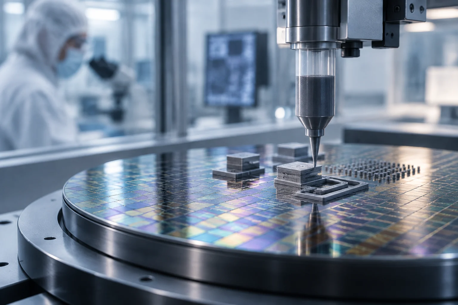
“3D printing of semiconductors” may suggest a machine that receives a design and delivers a ready-to-use chip. That image is too broad to describe the work covered by the sources consulted. The term can refer to printing inks containing semiconductor materials, building electronic components with three-dimensional geometry, or adding material layers through a controlled process. These activities share additive-manufacturing tools, but do not necessarily share materials, scales, or objectives. The phrase therefore needs context: the word printing alone does not reveal which process was used or what the process produced.
The label does not, on its own, identify which part of a device has been produced. In one case, the printed material might be an active layer; in another, the structure of interest might be a three-dimensional form that integrates several materials. And when the discussion is about prototyping, the aim may be to test a configuration or explore a structure, rather than to manufacture a component ready for sale. The method and the result should be described separately: knowing that printing was used is not enough to establish what function the object performs. A process name is not a complete description of either the device or its intended use.
It is also important to distinguish manufacturing an electronic device from producing the integrated circuits commonly called chips. An article about printed electronics may describe thin-film transistors or devices using two-dimensional materials without presenting an industrial route to manufacturing processors. Similarly, a nanomaterial-printing project does not, by itself, show that the resulting components meet commercial requirements for performance, volume, or reliability. These are different levels of analysis: demonstrating a principle, creating a prototype, and sustaining the manufacture of a product are not interchangeable or equivalent stages simply because they use additive techniques. Keeping these distinctions in view makes it easier to describe what a study establishes without implying that it answers questions about other technologies or stages of production.
Printing active materials is not the same as printing a chip
One example of printed electronics appears in a 2022 research article about devices manufactured entirely by inkjet printing. The title and bibliographic description identify the use of two-dimensional materials to form metallic, semiconductor, and dielectric layers. This supports describing an electronic device made with printed layers; it does not justify calling it a commercial processor or a general replacement for chip-manufacturing lines. The example is relevant to the question of how printed materials can be combined in an electronic device, but its scope should remain the one documented by the study.
Inkjet printing deposits material from an ink and forms patterns on a substrate. In an electronic component, different inks can serve different purposes. A metallic layer may form part of the connections, while semiconductor and dielectric layers perform other functions within the device. Combining materials makes it possible to build an electronic architecture, but does not automatically turn the result into a general-purpose integrated circuit. The available description identifies the classes of layers involved; on its own, it does not provide a complete industrial characterization of the device. In other words, the presence of several functional layers explains something about the device’s construction, not every aspect of its capability or production prospects.
The fact that a material performs a semiconductor function in a device is important, but it does not remove the other steps required to obtain a product: design, electrical contacts, packaging, characterization, defect control, and validation under operating conditions. These aspects help determine whether a device works reliably and whether it can be integrated into a particular application. They also make clear why evidence about the printed layers alone cannot settle questions about the complete product. The available sources do not provide a comprehensive industrial comparison between the study’s process and conventional integrated-circuit manufacturing. The laboratory example therefore does not support conclusions about general cost, capacity, or performance advantages.
Specify the object and its function
For that reason, it is best to reserve the term chip for the type of component that is actually documented. If the work examines an experimental architecture or printed electronics, the most accurate approach is to name it as such. The presence of a semiconductor material is a property of the device, not proof that a complete microprocessor has been printed. This precision does not diminish the research: it avoids attributing a scope different from the one described by the article and its results. Clear terminology recognizes the contribution while also keeping the claim within the evidence.
When reading a news item or technical summary, it can help to ask exactly what the sample consists of. Is the report about a layer, a component with a specific function, or an integrated system? Does “printed” refer to every part of the device or only to some of its layers? The answer helps distinguish a contribution involving materials or processes from a claim about manufacturing a complete chip. It is also useful to check whether the stated function belongs to the whole object or to one part of it. If the text does not specify these details, it is prudent to keep the description at the level the source actually supports.
Three-dimensional geometry and functional electronics
Another line of research uses three-dimensional printing to integrate materials and functions into shaped objects, rather than limiting itself to depositing flat patterns. A 2019 paper published in Nature Communications studies structured multimaterial filaments for printing optoelectronics. The interest of this approach lies in combining materials within a single printed structure; its documented scope concerns optoelectronics and, based on the title or available reference, it is not a demonstration of conventional chip manufacturing. The research illustrates that additive processes can be studied for structures in which the arrangement of materials is part of the design.
The practical difference is that printing can create connections or geometries that are difficult to achieve with a flat component. Manufacturing a three-dimensional form may be relevant when the spatial arrangement of materials is part of the device being studied. But geometry alone does not determine electronic performance or demonstrate that the structure can be produced uniformly. A shape can be an important part of a research result without, by itself, establishing how well the object performs across repeated production. The example illustrates a research direction in printed optoelectronics; it is not enough to attribute to it the capabilities of an advanced integrated circuit.
The existence of a functional printed structure does not automatically establish the integration density, manufacturing uniformity, or reliability required of an advanced integrated circuit. These are separate dimensions of the question “Can it be printed?”: manufacturable shape is only one; electrical performance, reproducibility, and intended use also matter. A result can be valid and useful for the specific application under study without meeting the requirements of other component types. Directly comparing technologies without clarifying the application can lead to conclusions that the sources do not support. The appropriate comparison depends on what each device is meant to do and which properties the relevant evidence actually describes.
What additive manufacturing describes
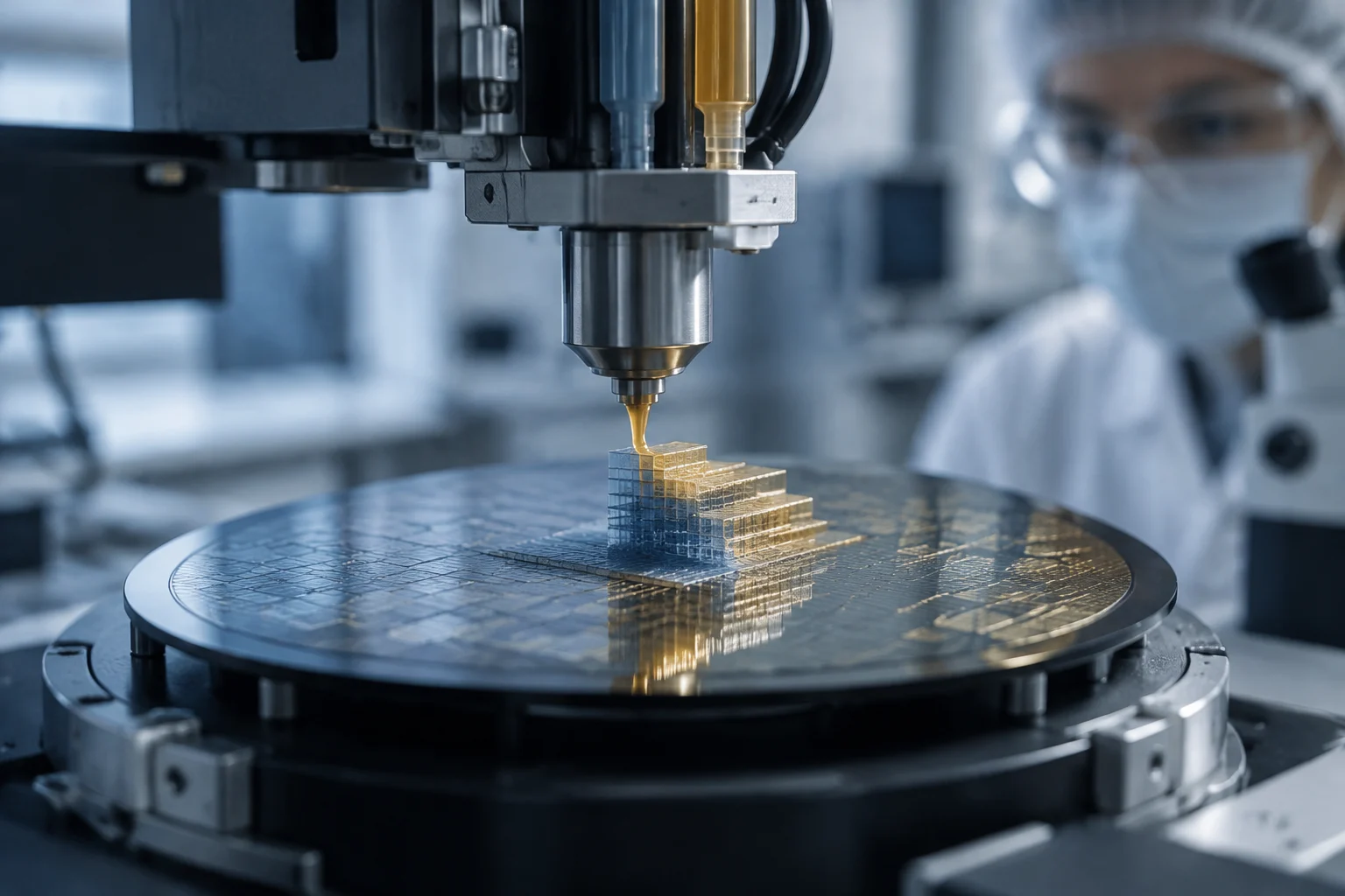
The term additive manufacturing broadly describes building a shape by adding material. It does not, by itself, specify whether the printed object is a semiconductor, an interconnect, an optical component, or a support element. Nor does it indicate the resolution achieved or the final function of the object. When assessing an announcement, it helps to check whether it explains the object’s electronic function, the materials involved, and the results measured. When that information is absent, the label “3D” says little about the device’s maturity. It identifies a broad approach to making an object, not a guarantee about the object’s completeness or readiness for use.
The same caution applies to expressions such as “printed electronics” and “printed device.” They can describe different combinations of substrates, layers, and processes; they do not, on their own, establish a production scale or level of integration. To interpret a result, it is better to focus on the specific description of the method and object presented, rather than assigning to one technique all the capabilities associated with other printing technologies. Asking what was made, how it was made, and what was measured keeps the description tied to the actual result instead of to a broad label.
Prototyping micro- and nanostructures
Prototyping projects offer another specific use, distinct from manufacturing chips in series. CORDIS presents the ATLANT3D project as aiming to develop an atomic-layer printer for the rapid prototyping of complex two- and three-dimensional structures at micro- and nanoscales. The European Commission’s results article describes the work as a proposal to facilitate the production of nanodevices. This framing supports describing research and prototyping; it does not justify turning the project into evidence that nanodevices are manufactured at mass scale. The stated objective and the demonstrated scale of production are different kinds of information, and should not be treated as interchangeable.
In this context, prototyping is an important word. It describes a development purpose: producing structures that make it possible to explore designs or advance device creation. It is not equivalent to claiming that a high-volume production line exists, or that the final device is already commercially available. The cited information places ATLANT3D in the development of a tool and the prototyping of small-scale structures. Keeping that scope explicit helps distinguish a research project’s objectives from the results that would be required to establish industrial deployment. A prototype can contribute to research without being a product intended for commercial manufacture.
Layer-by-layer deposition, including atomic layer deposition, should not simply be confused with a filament printer or an inkjet printer. Each method controls material and geometry differently. In this case, the CORDIS description focuses on layers and small-scale structures. The cited information available here does not provide a complete commercial-performance profile, production capacity, cost per part, or manufacturing yield for consumer products. Those gaps should not be filled with estimates or comparisons that the sources do not offer. Keeping the limits of the available description visible is more informative than implying that missing performance or production data are known.
Other printed-electronics applications
European research results also show that “printed electronics” includes applications broader than integrated circuits. A project documented by CORDIS addresses high-precision printing of electronics for thin-film transistors and large-area displays. Based on the focus indicated by its title, it is more accurate to treat it as a line of printed-electronics and thin-film-device research than to present it as processor manufacturing. The example broadens the picture of where printing methods are being explored without changing what the project description establishes.
This example is useful because it shows why a technique may be relevant to one family of applications without being suitable for every electronic component. The thin-film transistors and large-area displays named in the description belong to a different context from that of a commercial processor. The source documents the project’s approach; it should not be read as evidence that conventional chips were manufactured using that process. In general, identifying the specific application makes it possible to describe advances accurately without turning specialized research into a universal claim. It also keeps comparisons meaningful: a process discussed for displays should be understood in that context unless the evidence establishes a broader role.