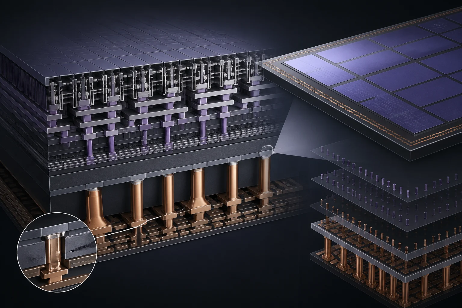
Why front-side PDNs are reaching their limits at 3 nm–2 nm
Conventional power delivery networks (PDNs) share the chip’s front-side wiring with signals. In very dense designs, this coexistence can increase congestion and make uniform voltage delivery more difficult. That is a reason to explore a different architecture, not proof that every 3 nm or 2 nm design has reached one single, inevitable limit.
The same interconnect region must accommodate distinct functions: carrying signals between blocks and supplying power to cells. Moving some power delivery to the backside can free front-side resources, but the effect depends on the architecture, cells, process, and workload. Improvements observed in one study therefore do not automatically transfer to every chip.
Separating the routes does not remove the need to design signal and power networks together; it changes where they are distributed. The practical question is whether this redistribution improves the balance among routing, power delivery, and timing in a particular design. A node name alone does not prove that a bottleneck exists or that a backside solution will solve it.
What BSPDN is and how it separates power from signals
A backside power delivery network (BSPDN) distributes power from the back of the silicon and connects it to device structures. The general aim is to reserve more front-side metal for signals and provide different routes for power. Integration details—including buried rails and vertical connections—vary by process; it should not be assumed that every solution uses the same structure.
Intel calls its backside power approach PowerVia. TSMC announced Super Power Rail for A16. These are names for industrial implementations, not synonyms for a universal specification. Separating routes can help reduce congestion, but does not by itself prove that every design will have less interference, lower voltage drop, or better margins.
Functionally, backside power delivery changes the path by which energy reaches the structures that need it; it does not mean that power and transistors are no longer electrically connected. The connection between the two sides remains essential. It is useful to distinguish the general architectural principle from process-specific details, without attributing results from one particular demonstration to every variant.
High-level manufacturing: sequences and trade-offs
Manufacturing a backside network requires integrating power connections with the back of the silicon and coordinating structures on both sides. Available sources describe elements of this architecture, such as buried rails and connection vias, but do not establish a complete industrial process flow that applies to every foundry.
A general description of BSPDN does not justify inferring an identical procedure at every fab. It is important to distinguish the principle—delivering power from the backside—from manufacturing details, which depend on the process and on what each manufacturer has published. Shared terminology also does not prove that implementations have the same steps, tolerances, or qualification criteria.
Integration must preserve the device’s electrical and mechanical reliability. Without verified sources on specific failure modes and controls, it is not possible to attribute particular defects, such as backside shorts, to every implementation or quantify their frequency. The lack of public detail does not demonstrate that a problem exists; it limits what can be stated rigorously.
Expected PPA improvements and what has actually been measured
Intel reported results from a PowerVia test vehicle: more than 90% cell utilization, about a 6% frequency improvement at comparable power, and more than a 30% improvement in voltage droop. These are company-reported figures for a demonstration, not independent measurements of a commercial product or a performance guarantee for every design. They should not be extrapolated to other nodes or manufacturers.
A practical reading requires separating test results from gains a customer might expect in a finished chip. Cell utilization, frequency, and voltage drop describe different aspects and depend on the measurement context. Without comparable studies covering diverse workloads, designs, and processes, there is no basis here for offering general improvement ranges for IR drop, Fmax, or core area.
Each figure answers a specific question. Cell utilization refers to occupancy of the area considered in the measured test vehicle; frequency compares an operating condition, while voltage droop describes a voltage variation. On their own, these figures do not establish power consumption, total area, or the performance of a complete product. A comparison is useful only when the reference design and measurement conditions are known.
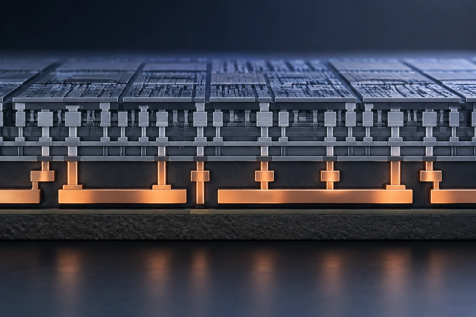
Status in 2026: what can be said about the announcements
Intel has presented PowerVia as a backside power technology and published results from a test vehicle. In addition, an academic paper documents a high-density SRAM fabricated using Intel 18A technology with PowerVia. This supports the claim that the technology has been demonstrated in structures associated with 18A; it does not, by itself, confirm use in a specific commercial product, its sale date, or that product’s performance.
TSMC announced A16 in 2024 with a backside power rail solution and a production outlook for 2026. This documents a plan communicated by the foundry; it does not confirm that volume production has begun or that the schedule has been met. Nor does it establish the architecture of other processes, such as N2 or N2P, without specific documentation.
A cautious answer to “who is implementing it in 2026” distinguishes demonstration, roadmap, and product: Intel has published evidence of PowerVia in a test vehicle and in an 18A SRAM; TSMC announced A16 with backside power and a 2026 production outlook. The sources verified here do not, on their own, confirm commercial availability of a specific product that would make the two cases equivalent.
Status in 2026: limits of information about other roadmaps
Information about SF2Z and its schedule comes from secondary technical coverage. It can be described as a roadmap according to that coverage, but not as confirmed availability or as proof that Samsung does—or does not—have products with backside power delivery. Dates and final characteristics can change, so this mention cannot establish definitive comparisons among manufacturers.
A secondary report about a roadmap does not have the same scope as confirmation of an available product. The evidence here also does not allow a planning horizon to be turned into a production commitment already fulfilled, or support the conclusion that undocumented public developments do not exist. The description is limited to the provisional nature of the reported information.
The general conclusion is that announced architecture, schedule, and commercial adoption must be assessed separately. For Intel, there is demonstration evidence; for TSMC, an A16 announcement and a production outlook; for SF2Z, secondary coverage of a roadmap. None of these categories should be confused with confirmation of availability or with product performance results.
Design and EDA impact: what an evaluation requires
A different power architecture requires power and signal routes to be considered together. Available sources do not verify tool or flow certifications for every process, or a single sign-off method. The availability of libraries, rules, and extraction models must be confirmed with the foundry and suppliers for the node in question.
A useful evaluation must use design resources corresponding to the specific process and check that the available tools and models cover the implementation being analyzed. Knowing that a backside architecture exists is not enough: interpreting results requires knowing the design conditions represented and what elements the analysis includes.
When evaluating a BSPDN proposal, check the conditions used to obtain performance figures and the type of test vehicle measured. It also matters whether data are process data, design estimates, or product results. This caution is especially important when PPA targets are reported rather than public manufacturing results. PPA brings together power, performance, and area as related dimensions, but a favorable figure in one does not automatically demonstrate an equivalent improvement in the others.