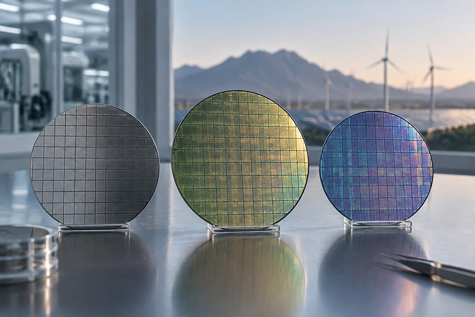
What a wide bandgap means
The bandgap is the minimum energy an electron needs to move from the valence band to the conduction band. In silicon, this value is about 1.1 eV; in silicon carbide (SiC), it is around 3.2 eV, and in gallium nitride (GaN), it exceeds 3.4 eV. This difference has practical consequences: it determines how well a material can withstand high electric fields without breaking down. That capability allows a device to block higher voltages and have lower leakage current at room temperature. These properties help explain why both materials are studied for power devices.
However, a wide bandgap does not automatically guarantee a superior device. For the theoretical advantage to translate into performance, the device structure, the quality of the gate–channel interface and the package’s thermal management also matter. Research from Oak Ridge National Laboratory (ORNL) notes that wide-bandgap semiconductors offer superior power switching features: high current density, low losses at high switching speeds and higher operating temperatures. These characteristics are fully exploited only when the device and its packaging are designed to support them. The material itself, therefore, does not determine the final performance; it is one part of a larger device and system design.
SiC and GaN: documented differences in use and operation
Silicon carbide has become established in high-power, high-temperature applications such as electric propulsion systems, power grids and renewable energy. Its thermal robustness and exceptional breakdown field make it the preferred choice when operation above 200 °C is required—a limit silicon cannot exceed. Gallium nitride, by contrast, excels in high-frequency switching and high efficiency. Its higher electron mobility facilitates miniaturisation and supports performance in radio-frequency devices and compact power supplies. These distinctions point to different areas of strength, rather than a single material being best for every application.
A comparative study published in Highlights in Science, Engineering and Technology in 2024 summarises this division: GaN leads in fast switching and high frequency, while SiC dominates in high power and high temperature. Silicon lags behind in these metrics, but remains relevant because its manufacturing base is mature and its cost is competitive. This specialisation reflects the intrinsic properties of each material as well as current limitations in heteroepitaxial fabrication. In particular, the immaturity of native GaN substrates has encouraged the development of solutions fabricated on silicon or SiC. The manufacturing context is therefore part of the technological comparison, alongside the properties of the semiconductor itself.
Comparable metrics in real components
To determine whether a wide-bandgap device outperforms silicon in a particular application, it is necessary to compare component-level metrics rather than material properties alone. The main metrics include blocking voltage, on-state resistance, maximum switching frequency, switching losses and thermal dissipation capability. Each describes a different aspect of operation, and its importance depends on the conditions in which the device is used. For example, a metric that matters greatly in one operating range may be less decisive in another. An ORNL report on 900 V and 1.2 kV SiC MOSFETs from four leading manufacturers shows that, in the intermediate-voltage range, these devices can reach currents of hundreds of amperes and switching frequencies far above those of silicon IGBTs, which are limited to a few hundred hertz at high voltages.
In diodes, characterisation of v-GaN diodes at Sandia National Laboratories found that, like SiC Schottky diodes, they have practically negligible reverse-recovery current compared with silicon PiN diodes. The result was obtained using a double-pulse test circuit. It matters because reverse-recovery losses are one of the main sources of inefficiency in hard-switching topologies. The table summarises the metrics and their practical relevance. It describes typical advantages associated with wide-bandgap materials, not a guaranteed outcome for every device or design:
| Metric | Practical relevance | Typical WBG advantage |
|---|---|---|
| Blocking voltage | Defines the operating voltage range | Higher in SiC and GaN |
| On-state resistance | Determines conduction losses | Lower in GaN at high frequency |
| Switching frequency | Affects the size of inductors and transformers | Higher in GaN and SiC |
| Reverse-recovery losses | Critical in hard-switching topologies | Practically negligible in SiC and GaN |
From the lab to the system: three levels of evidence
It is essential to distinguish among three levels of evidence: laboratory results, manufacturer specifications and benefits measured in complete systems. Experiments at Sandia or ORNL demonstrate a material’s potential under controlled conditions, but do not necessarily account for manufacturing variation, ageing or real environmental conditions. Manufacturer specifications describe nominal performance, although they often omit exact test conditions and process tolerances. Benefits observed in complete systems—such as an electric-vehicle inverter or a server power supply—offer a way to assess technical and economic viability in the final application. Each level answers a different question, so one should not be treated as a substitute for the others.
ORNL research on SiC power-module packaging for automotive applications shows why these levels should not be confused. Electrical and thermal performance gains are achieved by integrating single-sided cooling, three-dimensional planar electrical interconnection and double-sided direct cooling in a single packaging process. In other words, performance depends on how these features are brought together, not just on the semiconductor material used. Without such innovations, SiC’s material advantages do not translate into sufficient power density and efficiency to justify its cost. Packaging is as critical as the material: it connects the semiconductor’s properties to the thermal and electrical behaviour of the complete module.
Limits of the evidence and test conditions
Several factors prevent the advantages of wide-bandgap semiconductors from being generalised to every application. Switching-circuit design, package quality, substrate cost and long-term reliability are not captured by a simple comparison of material properties. An IEEE Spectrum article on the competition between GaN and SiC for green technology states that, whichever material wins, both will reduce greenhouse gas emissions by billions of tonnes. However, it does not specify the proportion of emissions or the applications involved. That limits the statement’s usefulness for making an engineering decision, where the scale and context of a claimed benefit matter.
Test conditions also vary significantly between laboratories and manufacturers, making it difficult to treat published figures as directly equivalent. For example, Sandia’s characterisation of v-GaN diodes used a double-pulse circuit whose parasitics limited the extraction of a significant recovery time. The result therefore does not allow a direct comparison with SiC data obtained under identical conditions. In addition, the immaturity of native GaN substrates introduces variability in defect density and affects reproducibility. These limitations do not invalidate the advantages of wide-bandgap materials, but they require a critical reading of published data and careful attention to how each result was obtained.
What independent verification is needed
To support current conclusions about the superiority of SiC or GaN over silicon, independent verification beyond manufacturer data is needed. This includes long-term reliability testing, such as assessments of mean time between failures (MTBF) and parameter degradation; comparisons under real operating conditions rather than nominal ones; and total cost of ownership analyses. Such assessments need to include packaging, cooling and system integration, because each can affect both performance and the viability of a solution. Considering these factors helps clarify whether a device-level advantage also matters in the system where the device will operate.
ORNL research on SiC and GaN devices with cryogenic cooling illustrates why environmental conditions matter. It shows that SiC MOSFET characteristics change significantly at cryogenic temperatures, with increased on-state resistance and slower switching. A result measured under one set of conditions is therefore not enough to describe performance under all others. In summary, the available evidence confirms that wide-bandgap semiconductors offer real advantages in specific power-electronics metrics, but those advantages are neither universal nor automatic. The choice between SiC or GaN and silicon must account for the material, device, packaging, system and operating conditions. A material property is necessary, but not sufficient: integration engineering determines the final benefit.