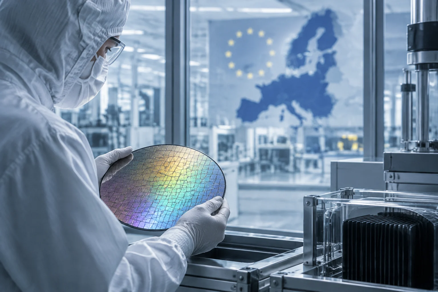
Backside power delivery is a chip-design approach that moves the network supplying electrical power to the rear of the silicon wafer. The goal is to keep that network from competing with the signal wires on the front side, where transistors communicate with one another.
The concept is attracting interest because advanced chips need dense wiring for both power and data. But it is not a universal performance upgrade: the outcome depends on how the backside connections are integrated, the chip design, and the manufacturing process.
Why move power to the back?
In conventional logic chips, transistors are built first, followed by layers of front-side wiring. Those metal layers carry signals between circuit elements and distribute power to them. As features and wiring become denser, the two jobs can compete for space, while resistance in the power network contributes to voltage drop across the chip.
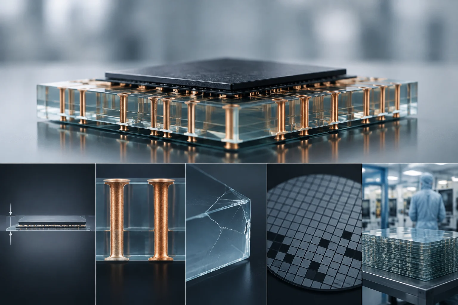
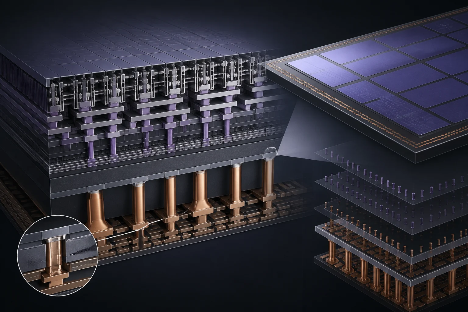
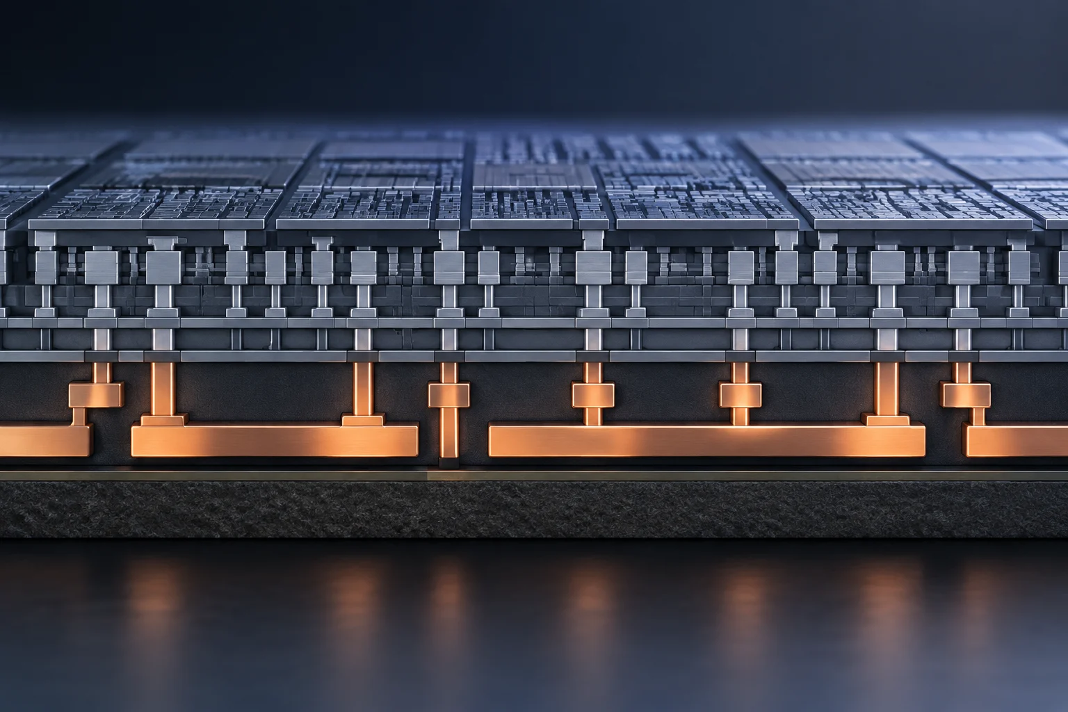
Backside power delivery separates those functions. Signal wiring stays on the front side, while power is routed through the wafer’s backside and connected to the transistors through vertical structures. Imec describes through-silicon vias (TSVs) as one way to bring power from the rear to front-side circuitry; specific designs can also use buried power rails within the chip.
The intended benefit is more room to arrange signal interconnects and a power path that can be designed with less resistance. This can help reduce voltage drop and ease wiring congestion, but those advantages depend on the implementation rather than following automatically from the label “backside power.”
The manufacturing trade-off
Moving power behind the wafer means adding process steps and new integration challenges. Imec identifies wafer thinning, very small TSV fabrication, accurate alignment between the wafer’s two sides, and protecting front-side devices during backside processing as important challenges.
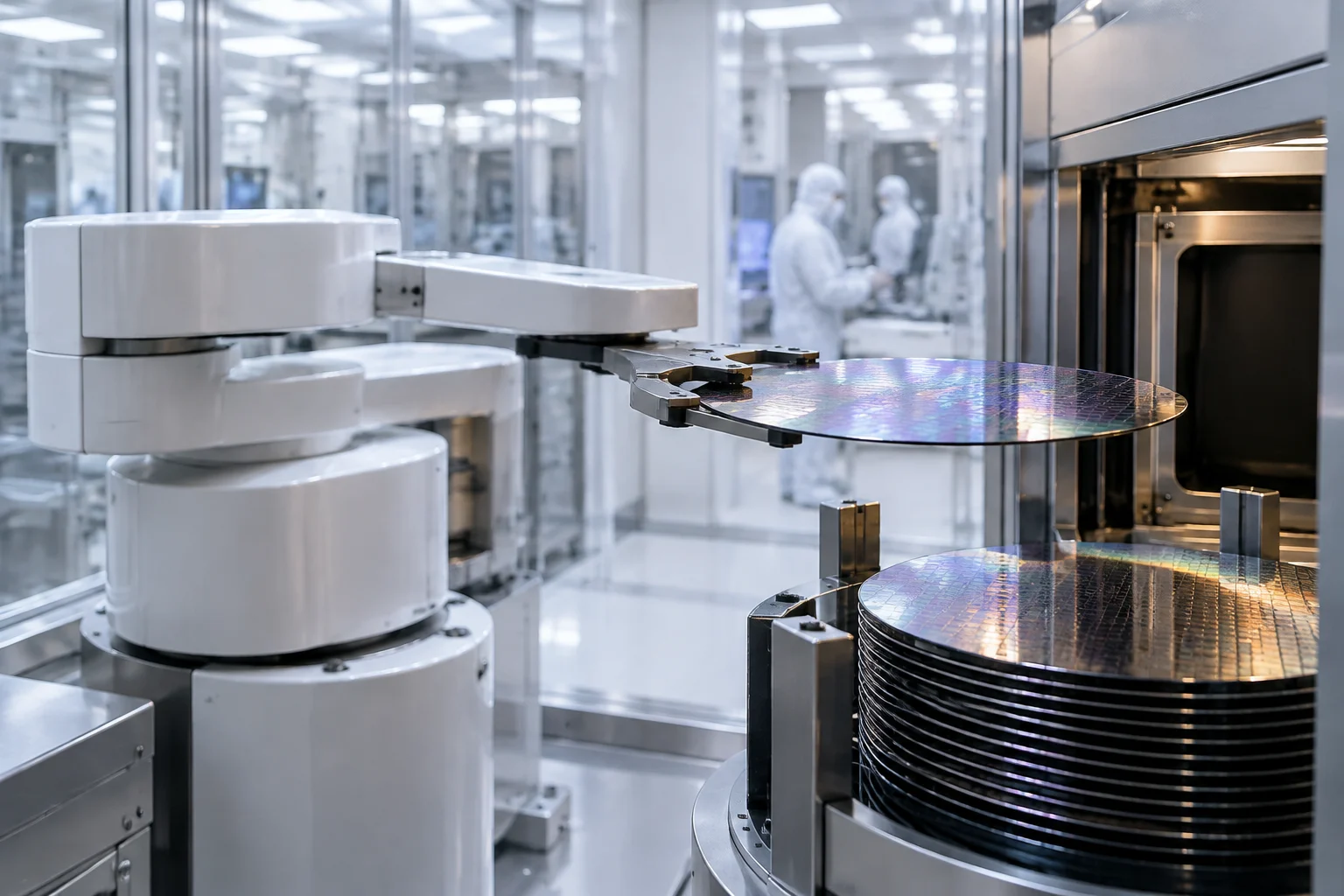
Intel’s PowerVia illustrates one manufacturing approach. Intel says it builds transistors and front-side interconnect layers, then flips and thins the wafer to expose a surface for backside power connections. That process can simplify crowded front-side wiring, but requires a more complex wafer flow and new ways to test the finished chip.
Testing is part of the engineering problem. With transistors embedded between front-side and backside structures, established debugging methods may not work unchanged. Intel reports developing and validating new debug techniques on its Blue Sky Creek test chip, including finding deliberately inserted errors.
Thermal behavior also has to be considered because the wafer’s silicon side normally contributes to heat dissipation. Intel says its test-chip work found transistor behavior close to that of its Intel 4 reference process despite the changes. That is a result reported for this test vehicle, not a guarantee for every backside-power design.
What the reported gains show
Intel reported that its Blue Sky Creek E-core test chip, built using Intel 4 transistors with a planned Intel 20A-style power and interconnect arrangement, achieved more than 5% higher frequency and over 90% cell density compared with its stated reference. The result demonstrates a design and manufacturing milestone; it is not a direct benchmark of a consumer processor against a competing product.
Imec and Arm evaluated a different implementation using design-technology co-optimization for a high-performance processor block. In that modeled comparison, a backside network connected through TSVs to buried power rails achieved 6% higher frequency and 16% smaller area than a front-side power network, with no reported energy-consumption penalty. Those figures are block-level evaluation results, not measurements from a mass-produced processor.
Imec also compared alternative ways to connect backside power to standard cells. Its study found that more direct backside connections could offer stronger scaling potential than some less compact approaches, while increasing integration complexity. Simulated ring-oscillator comparisons showed that the relative results varied with cell size and logic target; there is no single percentage that applies to all chips.
Who has announced or demonstrated it?
Intel has reported PowerVia test-chip results and identified the technology with its Intel 20A manufacturing plan. Intel’s 2023 announcement described Intel 20A production as expected in 2024; that historical plan should not be read as a current confirmation of the status of every product or process using backside power. Intel’s later Panther Lake announcement identifies that platform as built on Intel 18A, and does not by itself establish which backside-power features are present in a particular product.
Samsung announced that its SF2Z process would include an optimized backside power delivery network, comparing its expected power, performance, and area benefits with the first-generation SF2 node. Samsung scheduled SF2Z mass production for 2027. That is a roadmap commitment, not evidence that SF2Z was already in mass production when announced.
These announcements reflect different process roadmaps and implementations. Intel’s PowerVia, Samsung’s SF2Z plan, and the options studied by imec are all examples of backside power delivery, but their structures, manufacturing flows, and reported results should not be treated as interchangeable.
What to take away
Backside power delivery tackles a real scaling challenge by separating power distribution from front-side signal wiring. The clearest potential advantages are less front-side congestion and improved power integrity; the costs include additional process complexity, alignment and thinning requirements, and new testing and thermal considerations.
The reported gains are promising but need context: Intel’s figures come from a test chip, while imec and Arm’s comparisons come from design-level evaluation and simulation. Samsung’s SF2Z announcement describes a future manufacturing plan. The practical benefit will depend on the specific chip and process, not simply on whether a technology is described as “2nm” or as using backside power.