What designing a CPU with chiplets means
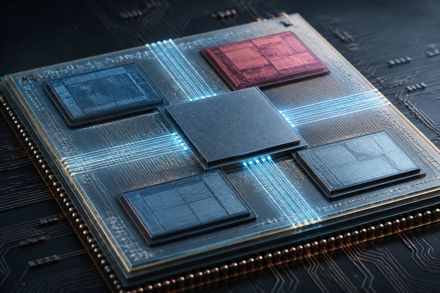
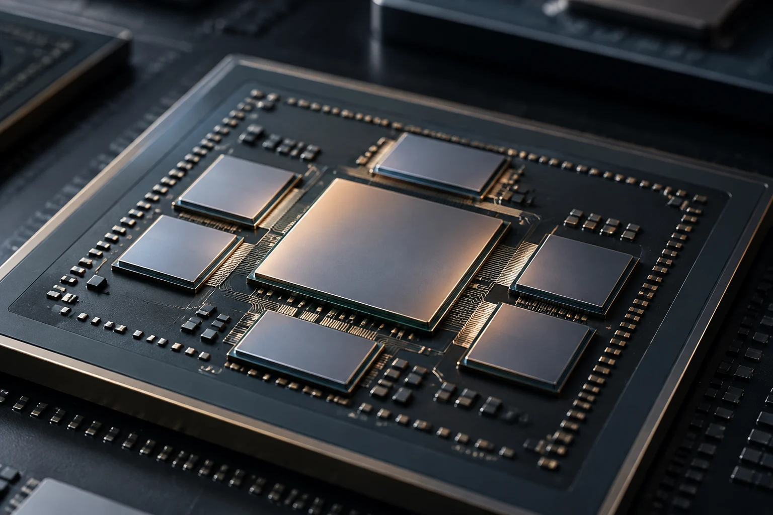
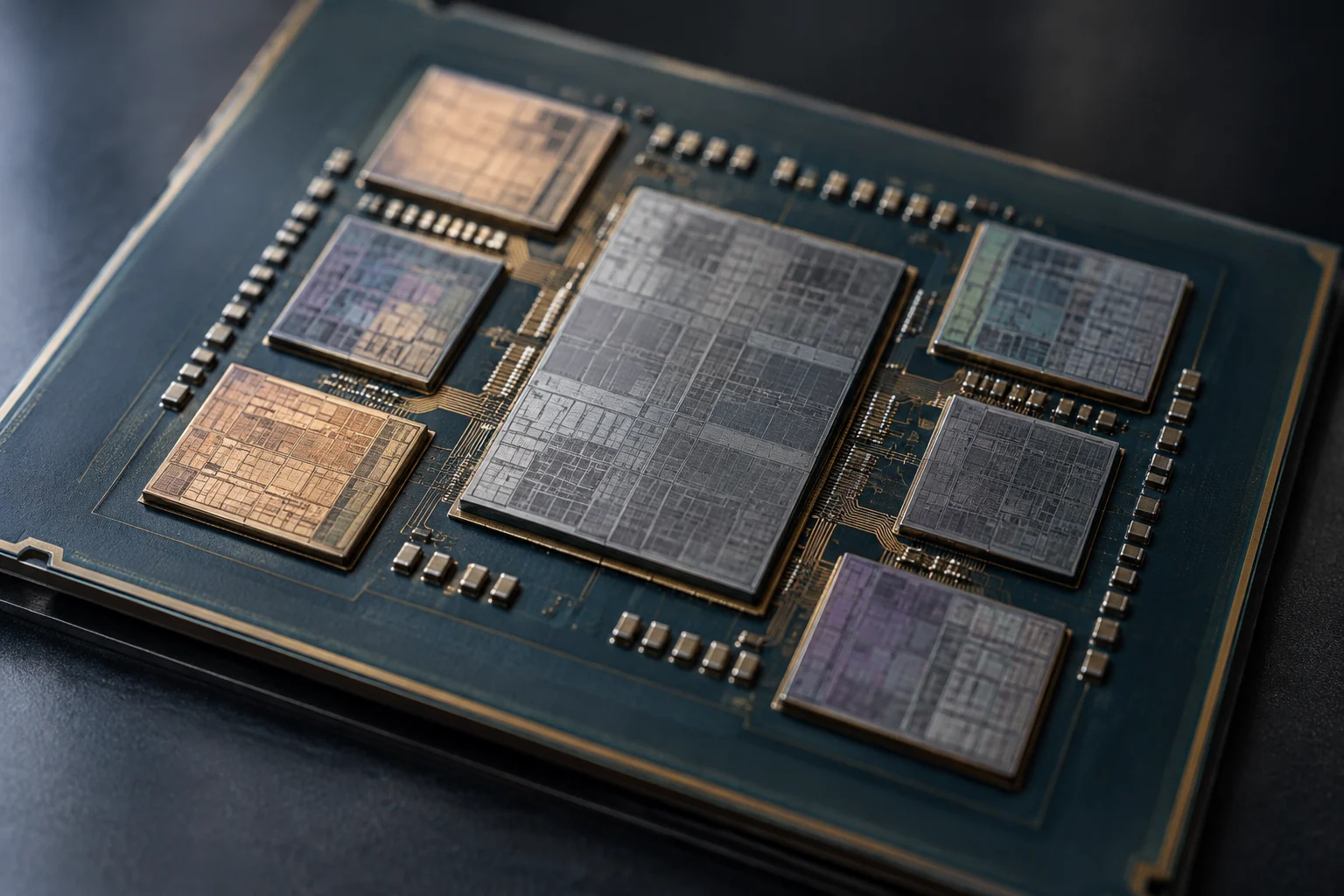
A chiplet processor assembles multiple silicon blocks—known as dies—within a single package. Instead of necessarily integrating all cores, caches, and input/output functions on a single monolithic die, the manufacturer distributes these tasks among interconnected pieces. Its physical organization is modular.
The key distinction lies between the complete package and each individual die. A chiplet is not a finished processor on its own: it requires a substrate or packaging structure, electrical connections, and mechanisms to exchange data and energy with other components. The specific distribution varies by architecture; it may separate compute and I/O, or combine compute blocks with blocks of different functions.
Modularity does not mean that all pieces are interchangeable. A design can reuse internal blocks or combine manufacturing technologies, but chiplets must fit a compatible architecture, interface, and assembly method. The goal is to decompose the design in a controlled way, not to assemble a CPU as if it were independent motherboard components.
Why separate silicon blocks
A large monolithic die can be difficult to manufacture: if a defect affects one area, it can render an extensive piece unusable. Smaller dies can reduce the impact of certain defects and allow the manufacturer to combine several blocks to create different configurations. It is a design and manufacturing opportunity, not a guarantee that every resulting processor will be cheaper.
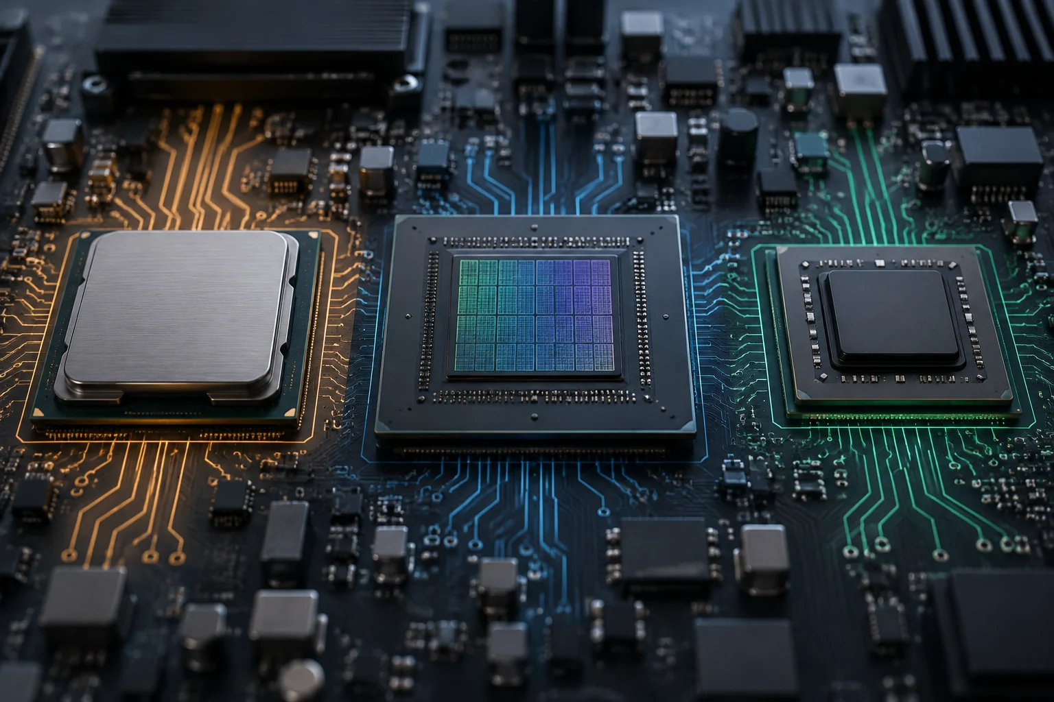
It is also possible to assign functions to different manufacturing processes. Compute blocks, which may benefit from a more advanced technology, do not have to share the same process with input/output circuits or other functions less sensitive to transistor density. This separation can help reuse designs and avoid migrating all components to the most expensive node; in exchange, it requires validating the interaction between pieces manufactured and designed separately.
Intel's technical documentation describes disaggregation as a way to combine chiplets and process nodes, noting that the size and function of blocks are chosen based on performance, area, and manufacturing. The final cost depends on the whole: number and size of dies, manufacturing yield, pre-assembly testing, packaging, and volume. Therefore, having a chiplet design is not enough to conclude that its production price will be lower.
Packaging is also part of the architecture
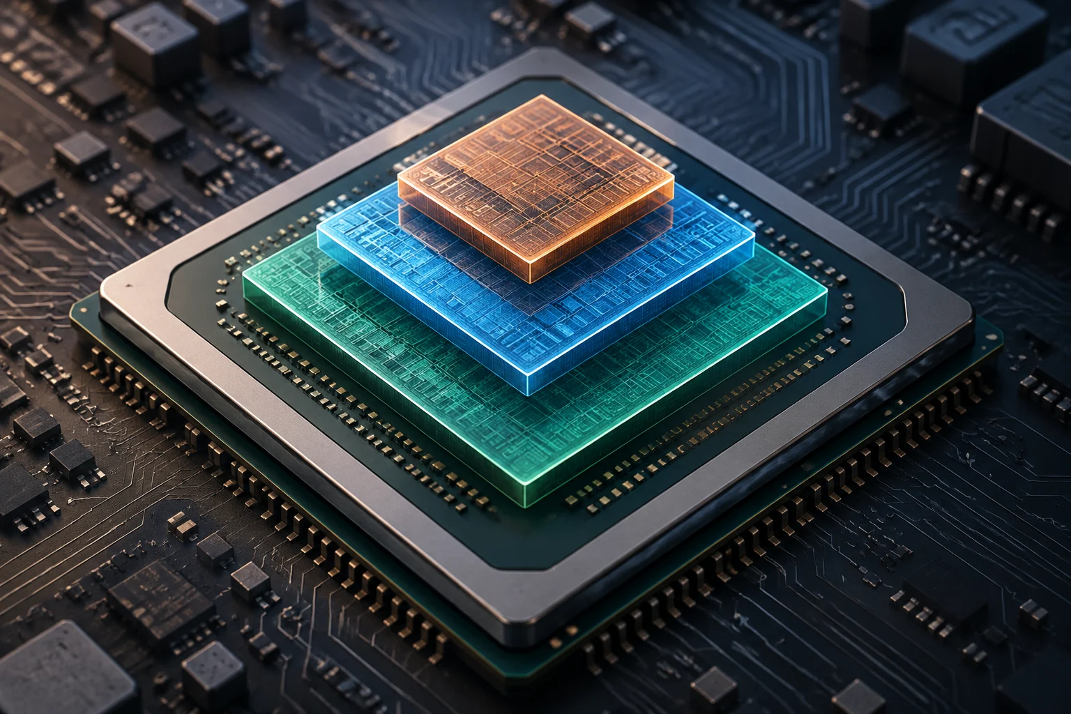
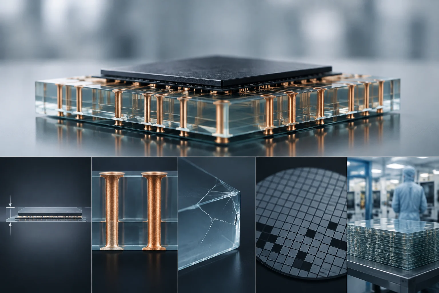
When multiple dies share a package, the way they are connected determines much of the design's potential. Some solutions place chiplets side by side and use bridges or interposers; others stack pieces vertically. Each option imposes different conditions for space, connection density, thermal dissipation, and manufacturing. The package is no longer a passive wrapper: it participates in the system design.
Interconnects must move data with sufficient bandwidth without consuming too much space or energy. They also add paths and physical limits: communication between blocks is not identical to what happens within a single die. Distance, link type, and the organization of caches and controllers can affect latency. A universal penalty cannot be assigned to all chiplet processors, as it depends on the implementation.
Intel's documentation presents technologies like EMIB and Foveros for connecting dies in 2.5D and 3D configurations. These are examples of industrial approaches, not a comparative performance measure between processors. Higher connection density does not automatically equal higher CPU speed: the benefit depends on what data crosses the link, how often, and what resources are available elsewhere in the system.
How chiplet design shapes a processor
A chiplet processor’s outcome depends on decisions across the design, package, and system—not on die count alone.
-
1 · Divide the design
Place selected functions on separate dies
-
2 · Select the package
Connect dies side by side or in a stack
-
3 · Plan communication
Balance connection density and system needs
-
4 · Judge the result
Evaluate the complete implementation
This summarizes design considerations, not a benchmark or a universal recipe; implementations differ by product.
Sources and references1
Interconnect, memory, and coherence
Compute blocks must communicate with caches, memory, and input/output functions. In some designs, memory controllers and external connections are on a separate die; in others, the organization is different. The placement of these elements determines the path a data takes and which blocks share resources. Therefore, counting chiplets or cores alone provides an incomplete picture of the architecture.
The interconnect transports data between blocks and can also carry control information. Its capacity and the protocol used condition the exchange between dies; if communication limits the data flow, adding compute units does not guarantee a proportional improvement in tasks that need to exchange results quickly. Performance depends on the implementation.
UCIe is a standard for interconnect between chiplets within a package. Its purpose is to define a common interface to facilitate modular designs and interoperability, although the existence of a standard does not mean any chiplet from any provider can be combined without further work: implementations, protocols, and system decisions must align. Interoperability is a design goal, subject to the technical and commercial conditions of each product.
Performance, cost, and power: what can be deduced
Architecture allows formulating hypotheses, not replacing measurements. Separating blocks can facilitate scaling the number of compute units or adapting manufacturing, but observed performance also depends on frequencies, cache, memory, thermal limits, energy, and workloads. A configuration with more dies may perform better in parallel tasks and not stand out in others where latency or single-core performance matters.
The same caution applies to performance per watt. A link between chiplets consumes energy, and the package must distribute power and evacuate heat. At the same time, a modular architecture can allow placing each function where it fits best and avoid manufacturing all parts with the most advanced process. The balance is established in the complete product, not just by counting how many blocks it contains.
To compare processors, it is advisable to use tests of the same task, with comparable configurations and conditions, and observe both performance and system power consumption. Architecture can help explain why two products behave differently, but it does not allow deducing a general advantage without measured results. Counting cores or chiplets is context, not a substitute for testing.
Software and scalability
Processor design and software determine how threads are executed on available cores. The application must also offer sufficient parallelism to take advantage of multiple cores: adding resources does not automatically convert a sequential task into a parallel one.
In a consumer computer, execution depends on the processor, operating system, and software, as well as the model and workload. Useful scalability depends on the work, not just on adding resources.
For a purchasing decision, the label 'chiplet' should not displace practical criteria: performance in the applications used, power consumption, temperature, price, compatible platform, and independent results. To interpret a technical sheet, it is advisable to treat the number of dies as a clue about internal organization, not as a direct classification of quality.
What to watch in the next generations
Packaging technologies and link standards help understand how systems with multiple dies are built. Industrial documentation features 2.5D and 3D interconnects and die-to-die interface proposals like UCIe. They are pieces of an architecture, not predictions that all manufacturers will adopt the same scheme or that the next generation will necessarily be faster or more efficient.
When evaluating an announcement, three questions are useful: what functions have been separated; what technology connects the dies and how memory and cache are organized; and what product tests show the effect on real applications. It is also interesting to distinguish a published standard from its specific implementation and an announced capability from a measured result. This reading avoids confusing more integration with an automatic improvement.
Chiplet design expands the options for manufacturing and organizing processors, but shifts part of the complexity to interconnect, packaging, and system coordination. Its value is demonstrated in each product: modularity and flexibility can be real advantages, while cost, performance, and power consumption require evaluation of the specific implementation.