The distinction that avoids confusing chip manufacturing with printing them
The expression «3D printing of semiconductors» can describe very different activities: manufacturing parts for machines that produce chips, building interconnections or encapsulations, or attempting to directly form electronic components using additive techniques. These are not equivalent stages nor do they have the same degree of maturity. The industrial evidence available in the sources reviewed here mainly supports the first group: the additive manufacturing of components for processing and lithography equipment. It does not demonstrate that a commercial printer produces a complete functional chip on its own.
This separation matters to those making decisions about electronic manufacturing processes. If the goal is to improve tools, fixtures, or machine components, 3D printing can be relevant as a part manufacturing method. If it is about replacing transistor fabrication on a wafer, the references provided do not certify that SLS or FDM are a production alternative. Presenting both cases as «printed chips» overstates what has been proven.
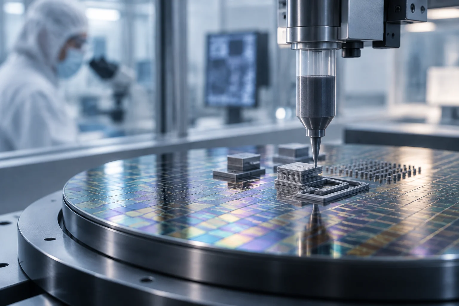
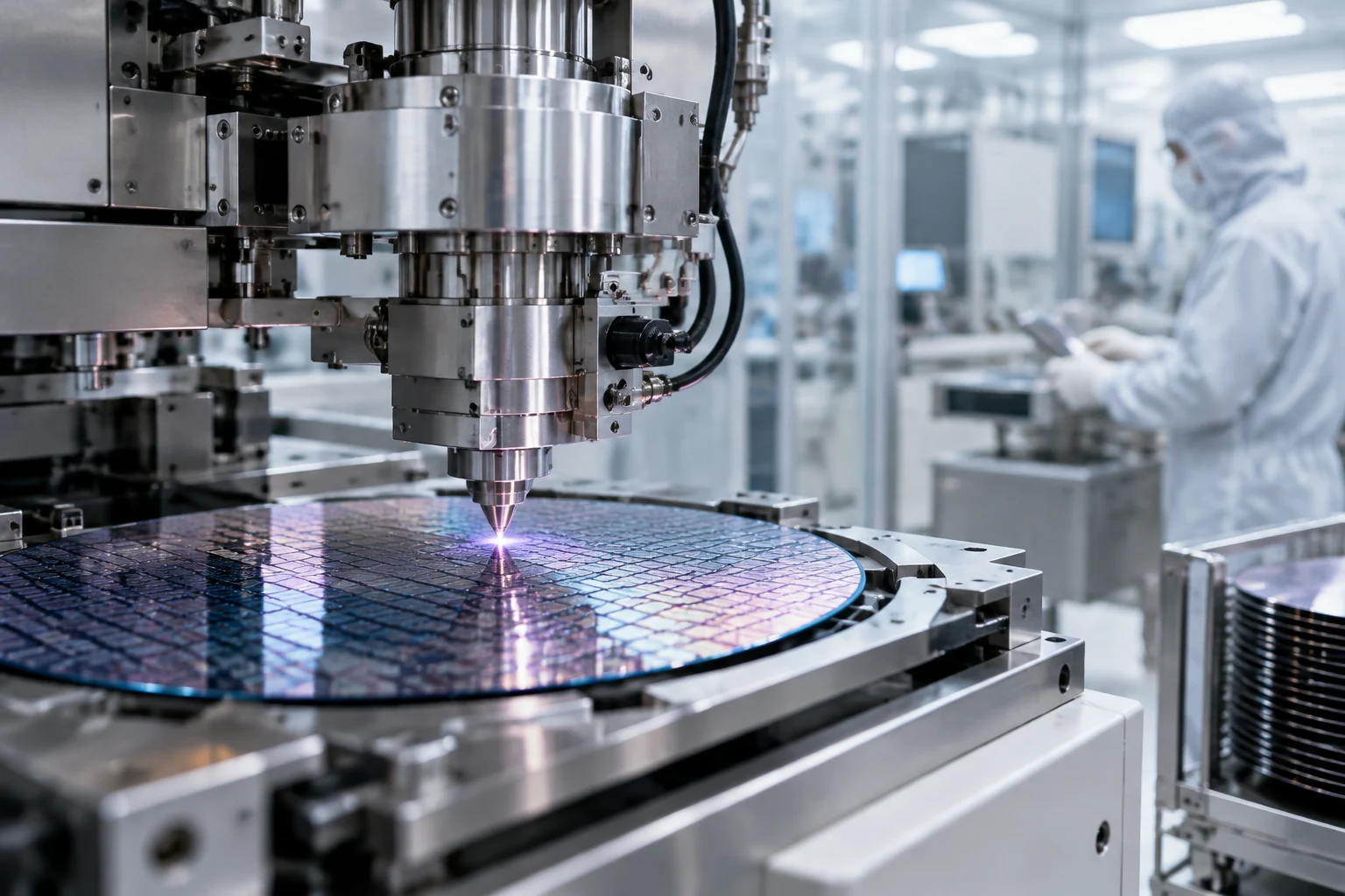
In the conventional industrial process, the chip is created through a sequence of steps on a wafer, with patterns and materials controlled at very small scales. Additive printing deposits or consolidates material to form geometries; by itself, that description does not establish that the resulting object has transistors, interconnections, and electrical performance comparable to an integrated circuit. The useful question is not whether 3D printing can intervene in semiconductors, but in which component and for what function.
The best-supported industrial use: parts for manufacturing equipment
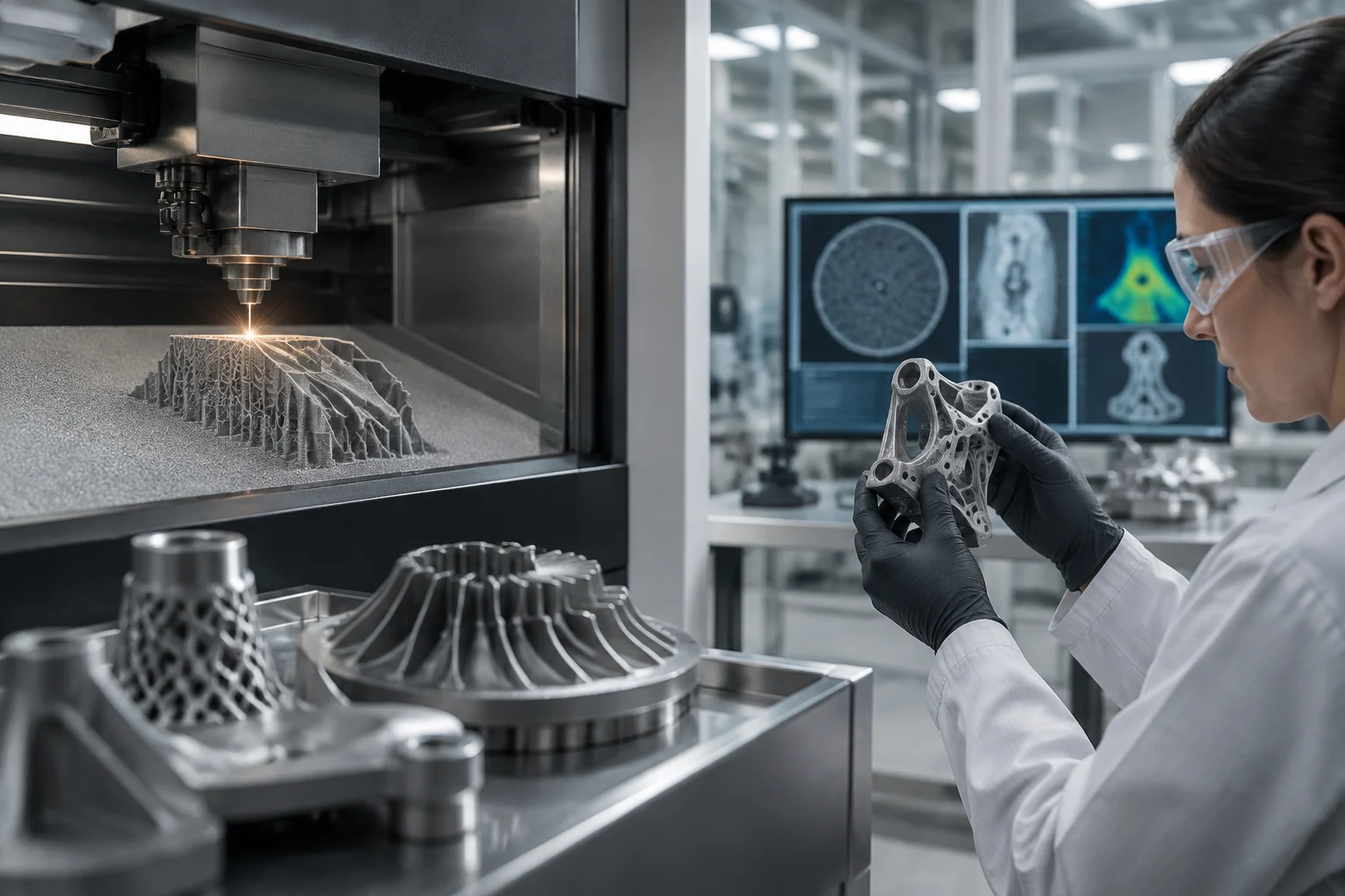
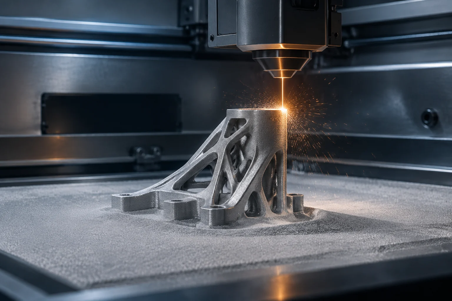
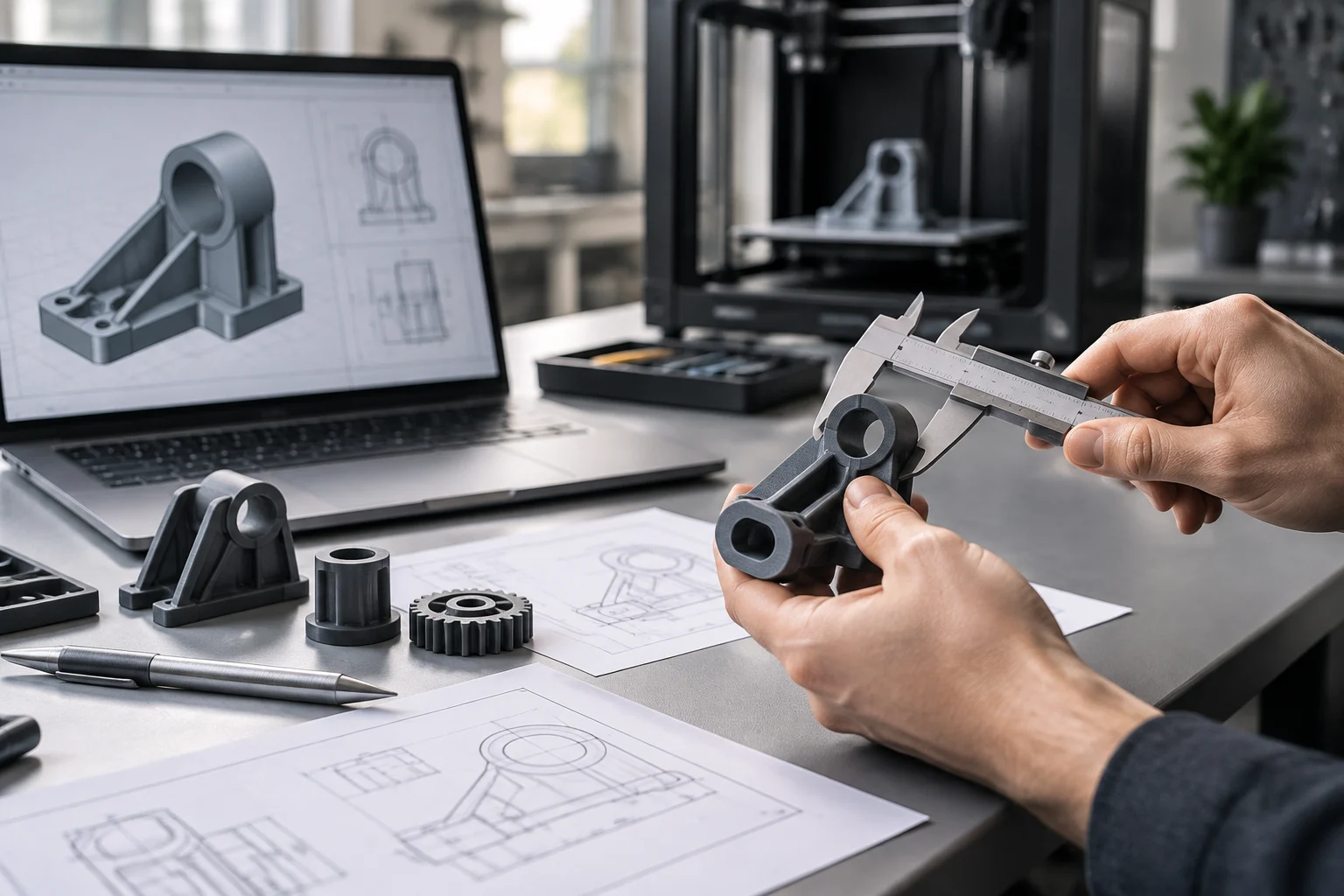
3D Systems describes applications of metal additive manufacturing intended for the capital equipment used in semiconductor production. The company presents application development services and support for moving from prototypes to production, and mentions areas such as thermal management. This places the use of 3D printing in the process machinery, not in the direct printing of integrated circuits. As it is material from the provider itself, it serves to document the type of application offered, but it does not constitute an independent validation of each reported result.
The company’s page announces equipment precision improvements of the order of 1 to 2 nm and five times greater stabilization. These figures should be read as commercial claims attributed to 3D Systems: in the available information, no specific equipment, complete methodology, comparison conditions, or external evaluation are specified. Therefore, they do not allow concluding that a 3D printing process generally raises chip manufacturing precision by that magnitude.
The practical distinction is relevant for engineers and plant managers. An additively manufactured part can be valuable if it meets geometry, stability, cleanliness, chemical compatibility, and repeatability requirements of the equipment where it is installed. The application must be validated part by part; the label «for semiconductors» does not by itself guarantee suitability for a clean room or for all stages of wafer production. The provided sources do not detail a universal qualification protocol or specify which part families meet each requirement.
SLS and FDM: manufacturing processes, not tests of printed chips
SLS —selective laser sintering— and FDM —fused deposition modeling— frequently appear in general explanations of additive manufacturing. In broad terms, SLS selectively consolidates powder material and FDM deposits molten thermoplastic filament layer by layer. The 3DZ reference describes FDM/FFF as filament extrusion and SLS as a 3D printing technology, but does not document that those techniques print integrated circuits. That a process can produce a three-dimensional part does not prove it can manufacture the functional elements of a chip.
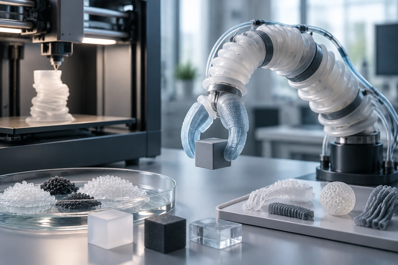
The case that often generates confusion is that of polymers with electrical properties or conductive additives. Aimplas presented in 2016 the development of compounds for 3D printing with semiconducting properties, in the context of materials for thermoplastic filament deposition. That reference certifies a line of material development, not a demonstration of transistor or complete chip production. Moreover, its age requires treating it as a precedent, not as a recent announcement or sufficient evidence of current industrial availability.
It is also worth distinguishing between conductor and semiconductor. A material that conducts electricity can serve for sensors, tracks, functional housings, or other components, but that is not enough to form a transistor. To demonstrate a functional semiconductor device, appropriate electrical and structural results are needed, in addition to identifying its architecture, process, and test conditions. Those categories should not be interchanged when evaluating a claim about printed electronics.
Metasurfaces and nanolithography: a distinct experimental line
Another line of research described in VoxelMatters coverage is holographic nanolithography of metasurfaces, presented as a technique that an academic and industrial team explores to manufacture electronic structures. The reference speaks of possibilities such as printed capacitors and adaptable encapsulations. It is a different approach from printing filament via FDM or consolidating powder via SLS: it relates to patterns and structures at the nanometer scale, not with a conventional polymer printer. It should not be attributed to SLS or FDM what that research proposes with another method.
The coverage identifies a research objective and potential uses, but does not provide detailed results here that allow comparing performance, production rate, manufacturing yield, reliability, or cost with current semiconductor processes. It also does not certify an industrial deployment of chip production via that method. Therefore, it is reasonable to describe it as a promising experimental path in its field, but not as technology already available to replace wafer fabrication.
A technical evaluation of such a proposal should seek, at a minimum, the scientific article or primary documentation, the materials and dimensions of the structures, the devices manufactured and their electrical measurements, the number of samples, and repeatability. It would also need integration results with circuits, stability, and compatibility with subsequent stages. A geometric demonstration is not equivalent to a qualified manufacturing process; without those data, its scalability cannot be judged.
What to require before talking about industrial production
For electronic manufacturing professionals, the investment question must be formulated at the application level: what component do you want to produce, what function does it perform, and what process requirement currently limits its manufacturing? The answers will differ for a machine tool, a support, a heat exchanger, a sensor, an encapsulation, or a chip. Available sources support that additive manufacturing can intervene in semiconductor equipment and that electronic materials and methods are being researched; they do not support a general conclusion of mass chip production by 3D printing.
Before accepting a production promise, it is advisable to request separate evidence for the material, the device, and the process. A functional prototype does not demonstrate repeatability; an electrical property of a sample does not demonstrate industrial performance; and a part manufactured for a semiconductor machine is not a semiconductor. A supplier evaluation should specify the method, tolerances, cleanliness, thermal stability, material compatibility, acceptance criteria, and results against a relevant reference.
A useful decision filter is to request documentation that allows answering these questions:
- What is printed: equipment part, functional material, electronic structure, encapsulation, or integrated circuit.
- With what process and material: naming SLS, FDM, or «additive manufacturing» is not enough; the specific combination needs to be identified.
- What has been measured: electrical, dimensional, thermal, and reliability performance, with conditions and method.
- At what stage it is: proof of concept, prototype, validation in equipment, or repeatable production.
- Who backs the result: manufacturer, research center, or independent evaluation, with accessible documentation.
Conclusion: real opportunity, but not in the usual sense of «printing chips»
3D printing already has a defensible industrial application in the semiconductor environment: producing components for equipment used in its fabrication, according to the offer documented by 3D Systems. On the other hand, there are precedents of material development with semiconducting properties and research proposals to manufacture electronic structures. They are advances of different nature and maturity, and the sources reviewed do not turn them into a production chain of printed chips.
For an engineering team, the practical decision is to separate opportunities for tools and auxiliary components —which can be evaluated with specifications and application tests— from promises to manufacture integrated circuits via SLS or FDM. Regarding the latter, the documentation available here does not certify industrial production, comparable performance, or replacement of conventional processes. The conclusion is not that additive manufacturing lacks utility in semiconductors, but that the term describes peripheral and experimental uses that should not be confused with printing a complete chip.
The most rigorous reading is, therefore, to speak of 3D printing for the semiconductor industry when manufacturing equipment parts, and reserve «printed semiconductors» for devices whose electronic function and process are demonstrated with verifiable data. That precision helps compare suppliers, avoid decisions based on ambiguous headlines, and orient validation toward the component that really needs to be produced.