Definition and Role in Silicon Quantum Architecture
Cryogenic CMOS refers to the operation of complementary metal-oxide-semiconductor integrated circuits at extremely low temperatures, generally below 10 K and, in advanced quantum applications, in the millikelvin range. This technology aims to solve one of the fundamental bottlenecks in quantum computing: the density of connections required to control and read each qubit. By placing control electronics near the qubit platform, interconnect line lengths are reduced, and external electromagnetic interference is minimized.
In silicon spin qubit architectures, the heterogeneous integration of cryogenic CMOS circuits allows universal logical operations to be performed directly at the cryogenic node. This approach differs from superconducting qubits, where control electronics usually remain at room temperature or 4 K, connected via coaxial cables that limit scalability. The promise of cryogenic CMOS is therefore a physical scalability that leverages silicon miniaturization to manage millions of qubits in a compact area.
It is crucial to distinguish between transistor operation at low temperatures and functional integration in a complete quantum system. While the former is well understood, the latter involves additional challenges of material compatibility, heat management, and electrical noise that can degrade qubit coherence. Recent literature shows that this frontier is being crossed, but with important nuances that we will analyze below.
Key Prototypes and Scientific Publications
One of the most significant recent milestones is the demonstration of spin qubit control using a CMOS chip operating at millikelvin, published in Nature. This work benchmarked silicon electron spin qubits controlled by heterogeneously integrated cryogenic CMOS circuits, showing that power density was low enough to allow scalability. The results indicated that millikelvin control has a minimal impact on one- and two-qubit gate performance, validating the technical viability of close integration.
In the Spanish academic sphere, the Electronic Design Group (GDE) at the University of Zaragoza and the Institute of Nanoscience and Materials of Aragon (INMA-CSIC) have published studies on the stability of polysilicon CMOS resistors against thermal cycles down to the deep cryogenic regime (4 K). These works confirm the stability of passive CMOS components under multiple cooling and heating cycles, an essential requirement for the long-term reliability of cryogenic systems.
Furthermore, technical presentations such as the one given by Alberto Gómez Saiz at the Polytechnic University of Madrid (UPM) in January 2026 detail a scalable multi-module architecture for a silicon spin quantum computer, fabricated with 22 nm FDSOI technology. Cryogenic measurements of key components were reported, including a 0-2 GHz SP8T switch and a 0.7 GHz low-noise amplifier (LNA), demonstrating the functionality of electronic interface blocks under real cryogenic conditions.
Technical Challenges: Noise, Heat, and Compatibility
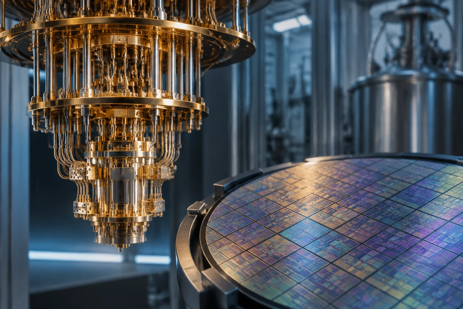
The main obstacle to the mass adoption of cryogenic CMOS is heat dissipation at the cryogenic node. Dilution refrigerators have a limited heat extraction capacity, so any power dissipated by control circuits reduces system efficiency and can raise local temperature, affecting qubit coherence. Current designs seek to minimize static and dynamic power, but this limits switching speed and integrated circuit complexity.
Another critical challenge is electrical noise. Spin qubits, especially in entanglement operations based on exchange coupling, are sensitive to electrical noise. The close integration of CMOS circuits can introduce switching noise that degrades quantum gate fidelity. Recent publications show that, with careful design and adequate control power, this effect can be mitigated, but it requires exhaustive characterization of each fabrication node.
Material compatibility is also a determining factor. Standard CMOS processes are not always compatible with the materials used in qubit fabrication, such as silicon-germanium heterostructures or quantum dots. Heterogeneous integration, which involves joining CMOS chips with qubit chips on the same substrate or in nearby modules, introduces packaging and alignment challenges that are still in the development phase. The uniformity and repeatability of these processes are essential to move from laboratory prototype to production.
Comparison with Room-Temperature Alternatives
The most common current alternative is to keep control electronics at room temperature or 4 K, connected to qubits via coaxial cables or waveguides. This approach is mature and well understood, but it suffers from a severe space limitation: each qubit requires multiple control lines, and the length of these cables increases with the number of qubits, limiting integration density and increasing latency and noise.
In comparison, cryogenic CMOS offers superior integration density, allowing more qubits to be controlled in a smaller area. However, this advantage is offset by design complexity and the need for cryogenic characterization. For small-scale applications (tens of qubits), room-temperature electronics remain more practical and economical. The transition to cryogenic CMOS is mainly justified when scaling to thousands or millions of qubits, where connection density becomes the limiting factor.
It is important to note that cryogenic CMOS does not completely replace room-temperature electronics, but complements the architecture. Hybrid systems, where high-level electronics (programming, synchronization) remain at room temperature and low-level electronics (qubit control) operate in cryogenics, are the most likely configuration in the short and medium term. This hybrid architecture allows leveraging the maturity of classical electronics and the density of cryogenic integration.
Time Horizon and Validation Metrics
The time horizon for industrial adoption of cryogenic CMOS in quantum computing is uncertain, but the signals are positive. The transition from laboratory prototypes to production systems requires overcoming non-trivial manufacturing, packaging, and characterization challenges. It is estimated that widespread adoption could occur in the 2030s, coinciding with the development of fault-tolerant quantum systems that require massive scalability.
To validate the progress of this technology, it is essential to observe specific metrics: the power density dissipated at the cryogenic node, the gate fidelity in the presence of nearby control circuits, and the repeatability of manufacturing processes. Reducing power per controlled qubit is a key metric, as it determines the system's thermal scalability. Likewise, the ability to fabricate cryogenic CMOS circuits with standard silicon processes, without costly modifications, is an indicator of economic viability.
In summary, cryogenic CMOS is a promising enabling technology for the scalability of quantum computing, but it is still in a technical demonstration phase. Current evidence supports its physical viability, but the distance to a robust and economical industrial implementation remains significant. Technology professionals should monitor advances in heterogeneous integration and thermal management to anticipate investment and development opportunities in this field.