The Problem Automation Solves
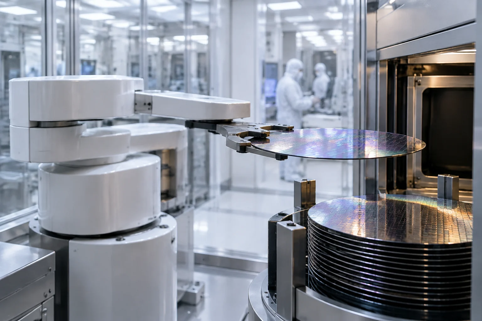
Semiconductor manufacturing is the most demanding manufacturing process in terms of cleanliness and environmental control. It is performed in isolated cleanroom environments where humidity, temperature, and particle contamination are monitored and controlled within specific parameters. Some processes require ultra-clean environments due to the sub-micron size of modern semiconductor devices, where contaminating particles can range from less than 10 nm to more than 100 µm.
Maintaining these conditions with human operators is difficult, and automation systems with moving parts are also sources of contamination. A primary motivation for highly automated factories is the replacement of humans with robots and other automation systems in cleanroom areas. The primary technical challenge is to minimize the number of particles generated by the robots and provide damage-free handling of wafers and other substrates.
Classification by Operating Environment
The operating environment has the greatest influence on the design, materials, and performance of a wafer handling robot. Robots are typically categorized into three main types: EFEM robots for front-end modules, vacuum transfer robots, and atmospheric handling robots. Each is designed for specific conditions within the production line.
EFEM robots operate in the atmospheric pressure front-end section of semiconductor equipment. They transfer wafers between load ports, aligners, and OCR readers before the wafers enter the process chamber. They are the bridge between factory automation and process equipment, optimized for continuous high-performance operation. Vacuum transfer robots operate inside vacuum process chambers and cluster tools, where wafers are moved between multiple processing modules without exposure to atmospheric contamination. They are designed for PVD, CVD, plasma etching, and vacuum metrology equipment.
Atmospheric handling robots operate outside vacuum chambers in standard cleanroom environments. They are commonly used for wafer inspection, storage, testing, and transport between processes. Their versatility makes them ideal for a wide range of semiconductor manufacturing and advanced packaging applications, including buffer stations and open cassette handlers.
Axis Configuration and Flexibility
Another important classification method is based on the number of axes or degrees of freedom of the robot. The number of axes determines its flexibility, range of motion, and accessible workspace. 3-axis robots provide basic linear and rotational motion suitable for relatively simple transfer tasks, offering a compact mechanical design and lower cost.
4-axis robots are the most commonly used configuration in semiconductor automation. By adding rotational flexibility, they offer greater accessibility without significantly increasing system complexity. They are the preferred choice in factories handling medium to high performance requirements, combining high precision with simpler mechanics. In 2024, 4-axis robots represented 30.2% of the wafer transfer robot market.
6-axis robots provide the highest level of flexibility and can reach complex positions from multiple orientations. They offer a large working envelope and the ability to avoid obstacles, making them suitable for custom equipment designs and R&D platforms. However, they require more sophisticated programming and motion control than lower-axis configurations.
Wafer-handling robot types by operating environment
The categories differ primarily in where they operate and which wafer-transfer tasks they perform.
| EFEM | Front-end atmospheric transfer |
|---|---|
| Vacuum transfer | Movement between vacuum modules |
| Atmospheric handling | Cleanroom transfer outside vacuum |
Applications vary by equipment design and production workflow.
Cleanroom Design Requirements
Being cleanroom-ready is not just a label, but the result of specific design decisions. For atmospheric robots, materials are chosen to reduce particle contamination from contact, friction, and outgassing. This includes stainless steel for critical moving parts, aluminum alloys for structural components, and plastics or composites like PEEK, PFA, and PTFE for parts that flex or contact substrates.
The robot's drive train is a significant source of particles during movement. Design guidelines include keeping all moving parts below the substrate, minimizing the number of moving parts, and evacuating generated particles. The use of cleanroom-compatible lubricants is recommended, which are chemically stable, non-toxic, and have low vapor pressure to minimize particle generation and outgassing.
For vacuum robots, challenges include providing the specified cleanliness and vacuum integrity in a vacuum cluster tool. The primary goal is to minimize the use of materials that outgas at or above the specified vacuum pressure. Dynamic vacuum barriers, which transfer motion from atmosphere to vacuum, use technologies such as magnetic drives, bellows, and magnetic couplings. The cost of these barriers can be significant depending on the specified vacuum pressure and the number of motion axes transferred to vacuum.
Factory Integration and Vibration Control
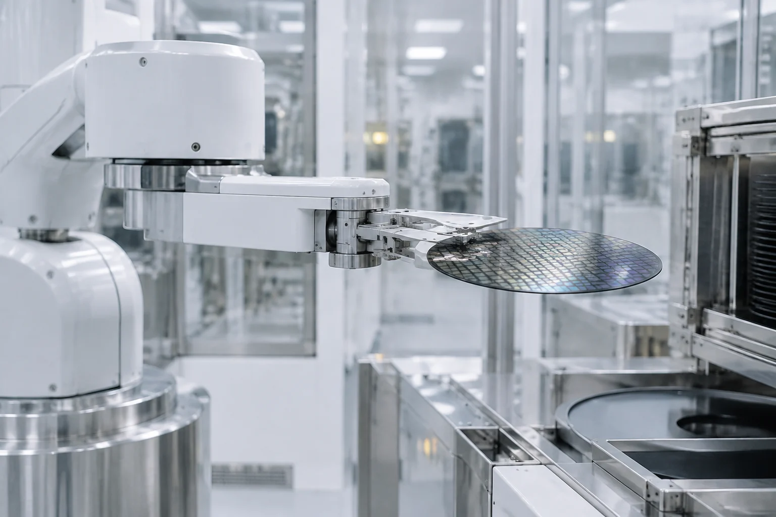
The wafer handling robot serves as the pivotal component of the wafer transfer system, where its operating speed and motion precision exert a direct influence on both the performance and productivity of wafer processing. With the advancement of semiconductor manufacturing toward nanometer-scale line widths and increased performance, the variable stiffness characteristics of flexible joints in wafer handling robots have become a critical challenge.
Wafer transfer systems need to achieve millisecond-level high-speed motion and sub-micron positioning accuracy in ultra-clean or vacuum environments to avoid wafer contamination or mechanical damage caused by vibration. Residual vibration and nonlinear dynamic behavior seriously restrict further performance improvement of the robot. Identifying the dynamic stiffness of flexible joints is fundamental to ensuring the motion performance of the system and significantly mitigating the impact of stiffness variations on system vibrations.
Integration with production systems is also crucial. Robots must interact with process equipment, perform loading and unloading, and coordinate with manufacturing systems. For example, EFEM robots integrate seamlessly with FOUPs, load ports, and aligners, optimized for continuous high-performance operation. The selection of the appropriate robot depends on several engineering factors, including the operating environment, wafer size and carrier type, equipment design, required performance, positioning accuracy, and available installation space.
Limits and Evaluation of Automation
Automation is not a universal solution that guarantees performance improvements in all applications. A documented application does not prove universal performance improvements, as performance depends on specific integration with process equipment and factory conditions. 6-axis robots, for example, offer exceptional versatility but also require more sophisticated programming and motion control, which can increase system complexity and integration time.
To evaluate an installation, indicators such as contamination, repeatability, transfer times, and availability under comparable conditions should be considered. Cleanroom compatibility, measured by ISO classes, is a key factor. In 2024, ISO Class 1 cleanroom-compatible robots represented 40.9% of the market, highlighting the strict control of contamination in advanced semiconductor manufacturing. Integrated robotic systems captured 50.5% of the market share, as factories seek greater automation and performance efficiency.
The global market for semiconductor wafer transfer robots reached $2.2 billion in 2024 and is projected to grow to approximately $5.35 billion by 2034, advancing at a CAGR of 9.3% between 2025 and 2034. This growth is driven by the increasing global demand for electronic devices, miniaturization, and advanced chips that increase the need for robots to handle larger wafers with precision. Automation of wafer handling supports higher yields by reducing wafer breakage and defects, directly impacting the efficiency and quality of semiconductor manufacturing.